
Graphene Raman Imaging and Spectroscopy Processing (GRISP) Software
GRISP is capable of giving accurate statistical data of key features of Raman spectrum of graphene over large areas, namely 2D, G and D peak intensity and ratios as well as 2D peak Full With at Half-Maximum. GRISP also maps processed data to form images from which growth quality can be easily visualized and quantified.
Available for online usage at nanohub.org/tools/grisp/
Parrish-Akinwande Graphene Field-Effect Transistor (GFET) Compact Model
(for linear and non-linear simulation studies)
ADS 2011 Graphene FET model (compatible with ADS 2011 and newer only)
ADS 2009 Graphene FET model (compatible with ADS 2009 and newer)
The models above afford the studies described in the publications below. Do cite the publications if the graphene model is employed in published work:
K. N. Parrish, M. E. Ramón, S. K. Banerjee, and D. Akinwande, “A Compact Model for Graphene FETs for Linear and Non-linear Circuit“, IEEE International Conference on Simulation of Semiconductor Processes and Devices (SISPAD), Denver, CO, USA, September 4, 2012.
K. N. Parrish and D. Akinwande, “An exactly solvable model for the graphene transistor in the quantum capacitance limit,” Applied Physics Letters, vol. 101, pp. 053501 (2012).
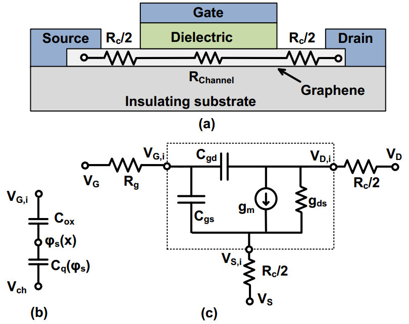
The inputs are summarized in the table below:
| Variable | Variable Name | Unit | Typical Values |
| Intrinsic quantities | |||
| Saturation Velocity | vsat | cm/s | 2.5e7 |
| Low-field mobility | Mobility (mu) | cm^2/V/s | 1000 – 10000 |
| Channel Length | Length (L) | um | < 10 |
| Channel Width | Width (W) | um | > 1 |
| Oxide Capacitance | Oxide_Cap (Cox) | fF/um^2 | 1-10 |
| Carrier Density | n (nimp) | 1/cm^2 | 1e11 – 5e12 |
| Extrinsic quantities (for all simulations) | |||
| Contact Resistance | Rc | Ω | 100-1000 |
| Drain Voltage | Vd | V | 0.1-5 |
| Gate Voltage | Vg | V | -5 to 5 |
| Dirac Offset Voltage | Vdirac | V | 0 |
The output for the simulation is drain current, which can be simulated in DC, S-parameter, harmonic balance, time-domain, or AC simulation. DC validation is shown below.
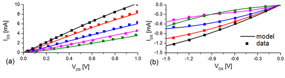
DC model validation with strong agreement between simulation (solid lines) and measured data (symbols) at several values of gate bias VGS, for GFETs with length (a) 100 nm (L. Liao et al) and (b) 10 µm (J. Kedzierski et al).