
Books

Carbon Nanotube & Graphene Device Physics
H.-S. Philip Wong and Deji Akinwande, Cambridge University Press, 2011.
Explaining the properties and performance of practical nanotube devices and related applications, this is the first introductory textbook on the subject. All the fundamental concepts are introduced, so that readers without an advanced scientific background can follow all the major ideas and results. Additional topics covered include nanotube transistors and interconnects, and the basic physics of graphene. Problem sets at the end of every chapter allow readers to test their knowledge of the material covered and gain a greater understanding of the analytical skill sets developed in the text. This is an ideal textbook for senior undergraduate and graduate students taking courses in semiconductor device physics and nanoelectronics. It is also a perfect self-study guide for professional device engineers and researchers.
Invited Talks
- D. Akinwande, “Bucked Atomic sheets: The Case of Phosphorene and Silicene”, Colloquium, Rice University, Dec. 2014.
- D. Akinwande, “Beyond the Flatlands: The Case of Phosphorene and Silicene”, Colloquium, Northwestern University, Nov. 2014.
- D. Akinwande, “Strain and Pressure in 2D Materials”, Seminar, Argonne National Lab, Nov. 2014.
- D. Akinwande, “2D Materials for Flexible Electronic Applications”, Nanotechnology for Defense conference (NT4D), Virginia, 2014.
- D. Akinwande, “Flexible 2d Nanoelectronics”, Colloquium, Case Western Reserve University, Sept. 2014.
- D. Akinwande, “Ubiquitous and Flexible 2D Electronics: Are the materials there yet?” Army Research Office Technical Exchange on 2D Materials and Nanoelectronics, Maryland, Aug. 2014.
- D. Akinwande, “Future and Prospects of 2D Materials”, DRC Rump Session, DRC Conference, June 2014.
- S. Chowdhury, L. Tao, S. Banerjee, and D. Akinwande, “Enhancement of Graphene Field Effect Transistor by Hexamethyldisilazane Surface Treatment.” IEEE Conference on Nanotechnology (IEEE-NANO), Aug. 2014.
- D. Akinwande, “Two-Dimensional Atomic Sheets for Heterogeneous Flexible High-Frequency and Low-Power Nanoelectronics,” SPIE Defense Micro and Nanotechnology Conference, May 2014.
- D. Akinwande, H-Y Chang, and J. Lee, “Flexible GHz Frequency and Low-Power Nanoelectronics Based on 2D Nanomaterials”, 225th ECS Meeting, Orlando, Florida, May 2014.
- D. Akinwande, “Pressure Induced Semiconducting to Metallic Behavior in MoS2 Crystals,” Colloquium, University of Pennsylvania, Philadelphia, PA, May 2014.
- D. Akinwande, “Wafer-scale graphene and Raman metrology,” 1st nanohub user conference, Phoenix, Arizona, April 2014.
- D. Akinwande, “Pressure induced semiconducting to metallic behavior in MoS2 crystals,” NRI e-workshop, March 2014.
- D. Akinwande, “Adventures In The Flatlands: The Rise of Flexible Atomic Sheets”, NSF-KAUST workshop on electronic materials, devices, and systems conference, KAUST, Saudi Arabia, February 2014.
- D. Akinwande, “Graphene for Terahertz Applications”, Rice University, October 2013.
- D. Akinwande, “The Silicon-rich and Flexible Futures of Graphene And 2D Atomic Sheets”, Colloquium, Princeton University, October 2013.
- D. Akinwande, “Adventures in The Flatlands: Progress and Prospects of Graphene And 2D Atomic Sheets”, Colloquium, University of Illinois at Urbana-Champaign, September 2013.
- D. Akinwande, “A Flexible Future for Graphene and 2D Nanoelectronics”, CMOSET Research Symposium, July 2013.
- D. Akinwande, “Electrons and holes in carbon nanotubes and graphene nanostructures”, Invited Tutorial, INFOS (Insulating Films on Semiconductors) Conference, Poland, June 2013.
- D. Akinwande, “ADVENTURES IN THE FLATLAND: FROM MATERIALS TO UBIQUITOUS SMART SYSTEMS”, Colloquium, Stanford University, May 2013.
- D. Akinwande, “Ubiquitous Smart Flexible Systems based on 2D Nanomaterials”, TechConnect Summit, May 2013.
- D. Akinwande, L. Tao, “Rethinking High-Performance CVD Graphene Nanoelectronics on Oxidized Silicon“, 223rd ECS Meeting, Toronto, Canada, May 2013.
- D. Akinwande, L. Tao, “Graphene-Si heterogeneous nanotechnology”, SPIE Defense Micro/Nanotechnology Conference, April 2013.
- D. Akinwande, J. Lee, S. Chang, L. Tao, “Two-Dimensional Atomic Sheets for Low-power Flexible, Wearable Nanoelectronics”, MRS Spring Conference, April 2013.
- D. Akinwande, “2D Flexible Nanomaterials & Nanoscience for Defense technology,” nanoMonterrey Conference,, Mexico, Nov. 2012.
- D. Akinwande, “Ubiquitous Smart Systems: A Revolution in the Making,” Sematech IEDM CMOS and Beyond Workshop, San Francisco, Dec. 2012.
- D. Akinwande, “Adventures with 2D Atomic Sheets and Plastic Nanoelectronics: New Research Directions and Applications“, 3M Science and Engineering Faculty Day, Minnesota, Nov. 2012.
- D. Akinwande, “Towards Large-Scale Graphene Technology and Electronics,” Army ARL Workshop, MD, Sept. 2011.
- D. Akinwande, “Adventures with Carbon Nanomaterials and CMOS: New Research Directions,” Silicon Labs, Austin, TX, June 2011.
- D. Akinwande, ” Adventures with Nanoelectronics: New Research Directions,” Texas Instruments, Dallas, TX, Dec. 2010.
- D. Akinwande, “Carbon Nanotubes for Flexible Electronics”, NSF Workshop, Arlington, VA, October 2010.
- D. Akinwande, “Adventures with Exploratory Technologies: Carbon Nanotechnology and Bio-Nanotechnology,” University of California, Davis, Davis, CA, March 2009.
- D. Akinwande, “Adventures with Carbon Nanotubes: Device Physics, Material Science, and Analog Circuits,” University of California – Berkeley, February 2009.
- D. Akinwande, “Adventures with Carbon Nanotubes: History, Applications, Science & Technology,” Integrated Circuits Seminar, Stanford University, Stanford, CA, Jan. 2009.
- D. Akinwande, “Adventures with Carbon Nanotubes: Analog Circuits, Material Synthesis, and Device Modeling,” Rochester Institute of Technology (RIT), Rochester, NY, Sept. 2008.
- D. Akinwande, Ada Poon, Teresa Meng, H.-S. P. Wong, “Adventures with Carbon Nanotubes: 3D Inductors, Capacitors & Antennas, and THz ICs”, Army Workshop, ARL, Maryland, August 2008.
Journal Papers
2021
- Yuqian Gu, Martha I. Serna, Sivasakthya Mohan, Alejandra Londoño-Calderon, Taimur Ahmed, Yifu Huang, Jack Lee, Sumeet Walia, Michael T. Pettes, Kenneth M. Liechti, Deji Akinwande
“Sulfurization Engineering of One-Step Low-Temperature MoS2 and WS2 Thin Films for Memristor Device Applications”; Advanced Electronic Materials, October 2021.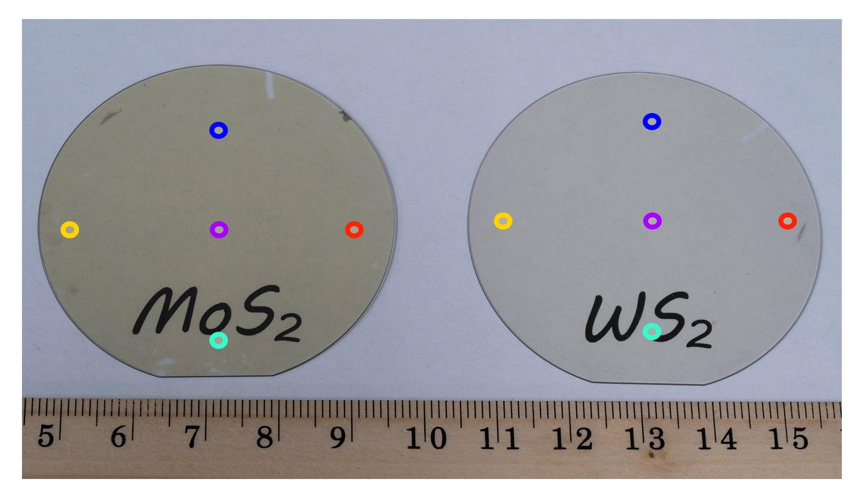
- Sabeen Fatima, Xu Bin, Mohammad Ali Mohammad, Deji Akinwande, Syed Rizwan
“Graphene and MXene Based Free-Standing Carbon Memristors for Flexible 2D Memory Applications “; Advanced Electronic Materials, September 2021.
- Seongin Hong, Haewon Cho, Byung Ha Kang, Kyungho Park, Deji Akinwande, Hyun Jae Kim, and Sunkook Kim
“Neuromorphic Active Pixel Image Sensor Array for Visual Memory”; ACS Publications, August 2021.
- Otitoaleke Akinola, Isha Chakraborty, Hugo Celio, Deji Akinwande & Jean Anne C. Incorvia
“Synthesis and characterization of Cr2C MXenes”; SpringerLink, June 2021.
- Leslie Valdez-Sandoval, Eloy Ram ́ırez-Garcıa, Saungeun Park, Deji Akinwande, David Jimenez, Anibal Pacheco-Sanchez
“A small-signal description of black phosphorus transistor technologies for high-frequency applications”; IEEE Xplore, June 2021.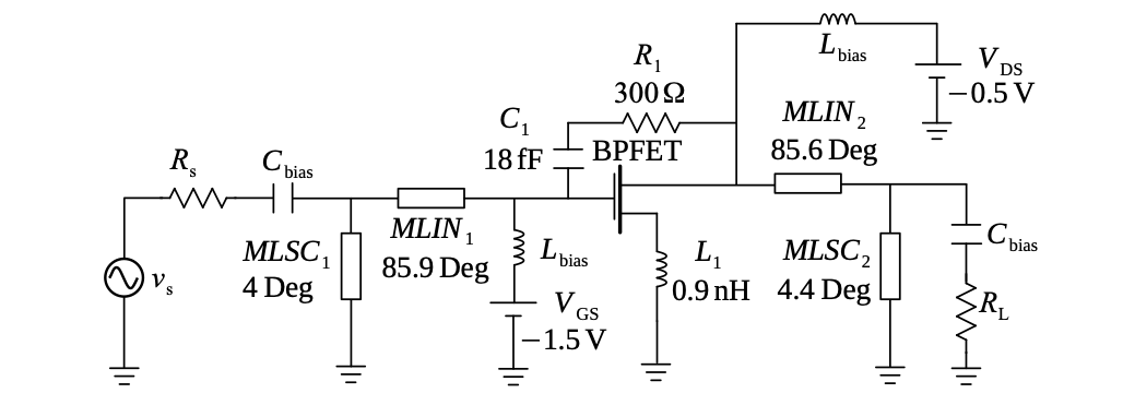
- Md Hasibul Alam, Sayema Chowdhury, Anupam Roy, Maria Helena Braga, Sanjay K. Banerjee, and Deji Akinwande
“Direct growth of MoS2 on electrolytic substrate and realization of high-mobility transistors”; APS Physics, May 2021.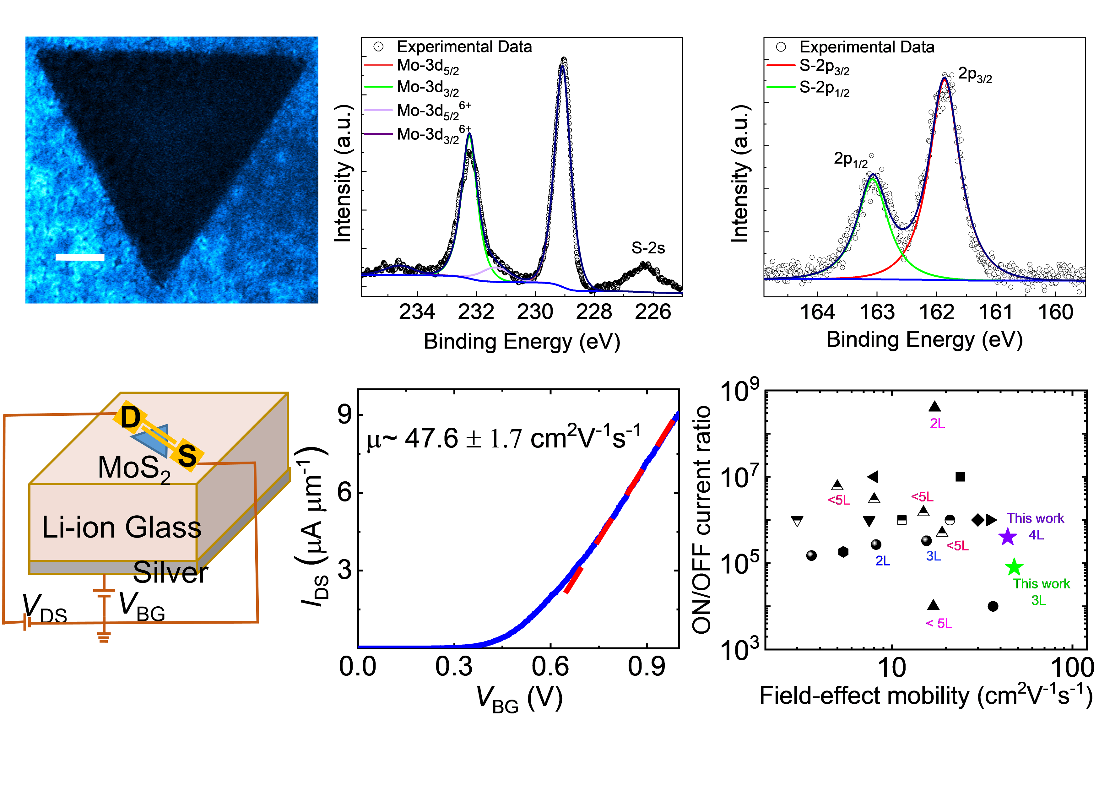
- Zilong Wang, Patrick Altmann, Christoph Gadermaier, Yating Yang, Wei Li, Lavinia Ghirardini, Chiara Trovatello, Marco Finazzi, Lamberto Duo,̀ Michele Celebrano, Run Long, Deji Akinwande, Oleg V. Prezhdo, Giulio Cerullo, and Stefano Dal Conte
”
Phonon-Mediated Interlayer Charge Separation and Recombination in a MoSe2/WSe2 Heterostructure”; Nano Letters, February 2021.
- Zhaoying Dang, Wenhui Wang, Jiayi Chen, Emily S Walker, Seth R Bank, Deji Akinwande, Zhenhua Ni,and Li Tao
“Vis-NIR photodetector with microsecond response enabled by 2D bismuth/Si(111) heterojunction”; 2D Materials, IOPscience March 2021.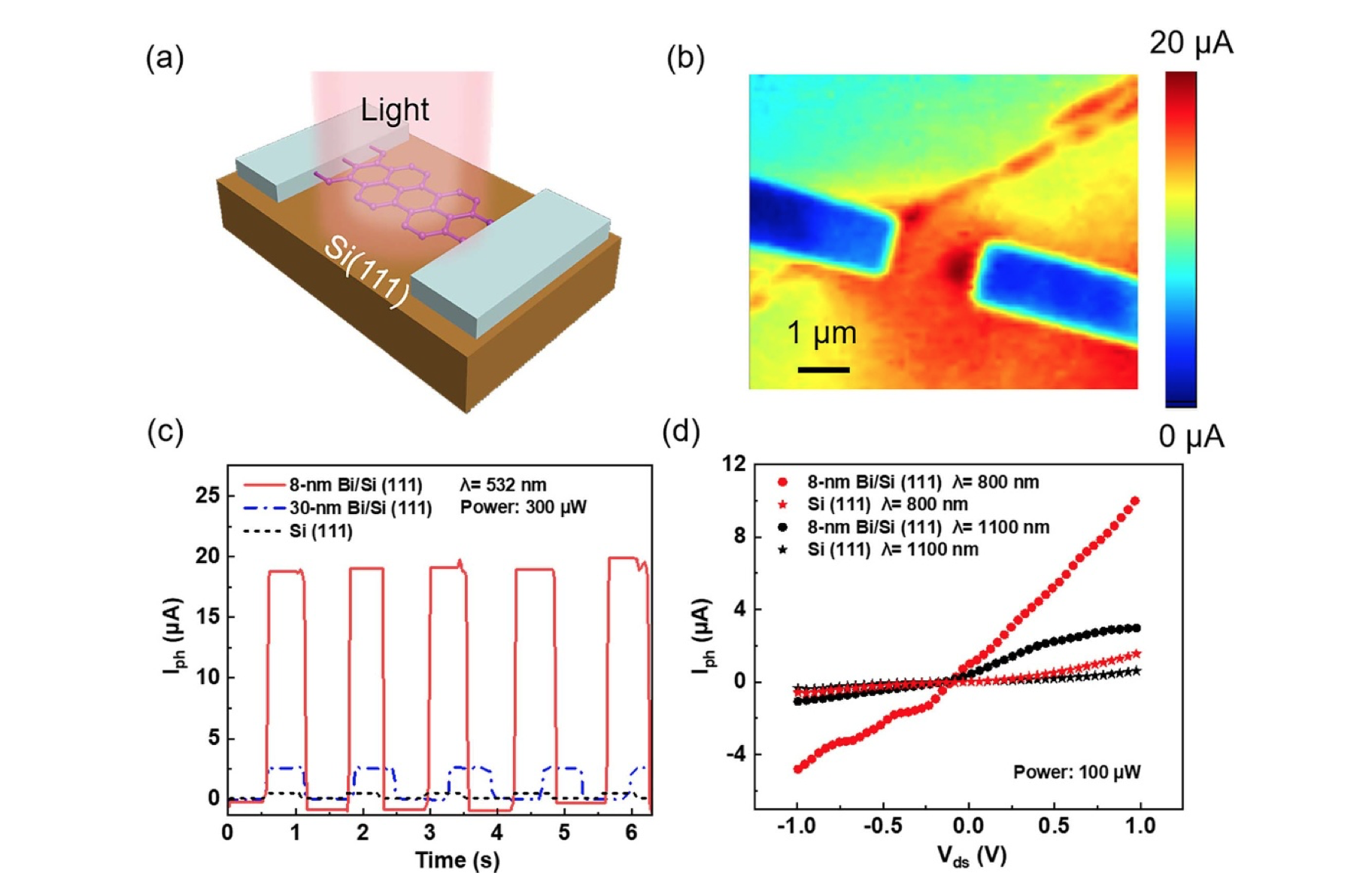
- Dmitry Kireev, Shideh Kabiri Ameri, Alena Nederveld, Jameson Kampfe, Hongwoo Jang, Nanshu Lu & Deji Akinwande
“Fabrication, characterization and applications of graphene electronic tattoos”; Nature Protocols, April 2021.
- Vaishakh Kedambaimoole, Neelotpala Kumar, Vijay Shirhatti, Suresh Nuthalapati, Saurabh Kumar Mangalore Manjunatha Nayak, Prosenjit Sen, Deji Akinwande, Konandur Rajanna
“Reduced Graphene Oxide Tattoo as Wearable Proximity Sensor”; Advanced Electronic Materials, March 2021.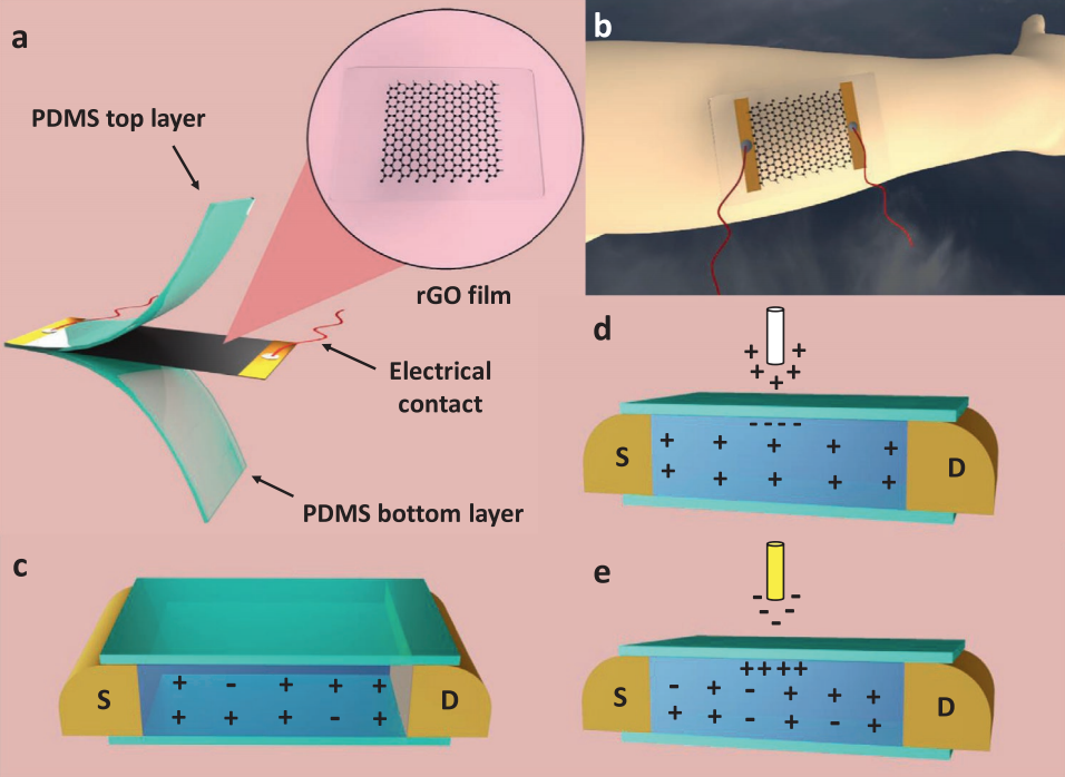
- Beibei Zhu, Qichao Chen, Siyao Jiang, Milo Holt, Weinan Zhu, Deji Akinwande, Li Tao
“Thermoelectric effect and devices on IVA and VA Xenes”; InfoMat Early View, January 2021;.
- Dmitry Kireev, Emmanuel Okogbue, RT Jayanth, Tae-Jun Ko, Yeonwoong Jung, and Deji Akinwande
“Multipurpose and Reusable Ultrathin Electronic Tattoos Based on PtSe2 and PtTe2”; ACS Nano January 2021;.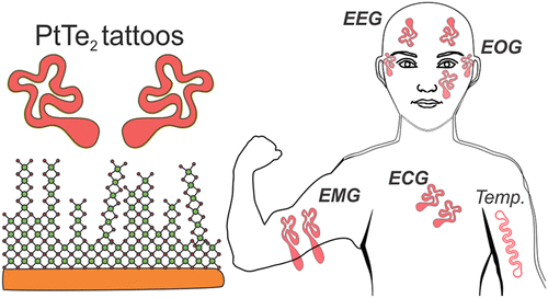
Journal Papers
2020
- Ruijing Ge, Xiaohan Wu, Liangbo Liang, Saban M. Hus, Yuqian Gu, Emmanuel Okogbue, Harry Chou, Jianping Shi, Yanfeng Zhang, Sanjay K. Banerjee, Yeonwoong Jung, Jack C. Lee, Deji Akinwande
“A library of atomically-thin 2D materials featuring conductive-point resistive switching phenomenon”; Adv. Mater., Dec. 2020;.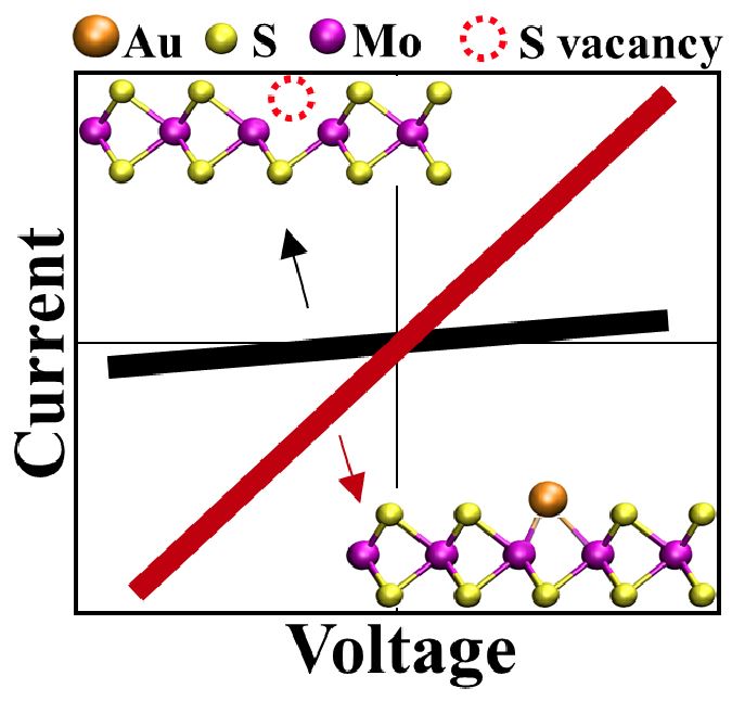
- Xiaohan Wu, Ruijing Ge, Yifu Huang, Deji Akinwande and Jack C. Lee
“Resistance state evolution under constant electric stress on a MoS2 non-volatile resistive switching device”; RSC Advances, November 2020;.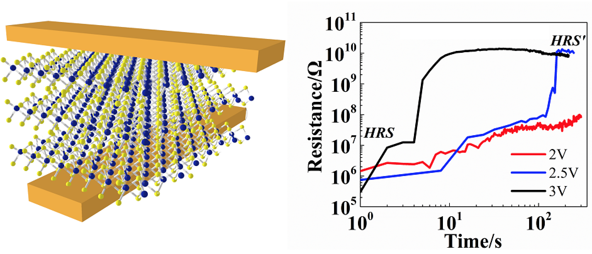
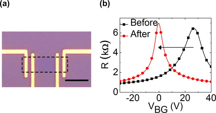
- Saban M. Hus, Ruijing Ge, Po-An Chen, Liangbo Liang, Gavin E. Donnelly, Wonhee Ko, Fumin Huang, Meng-Hsueh Chiang, An-Ping Li & Deji Akinwande
“Observation of single-defect memristor in an MoS2 atomic sheet”; Nature Nanotechnology, November 2020;.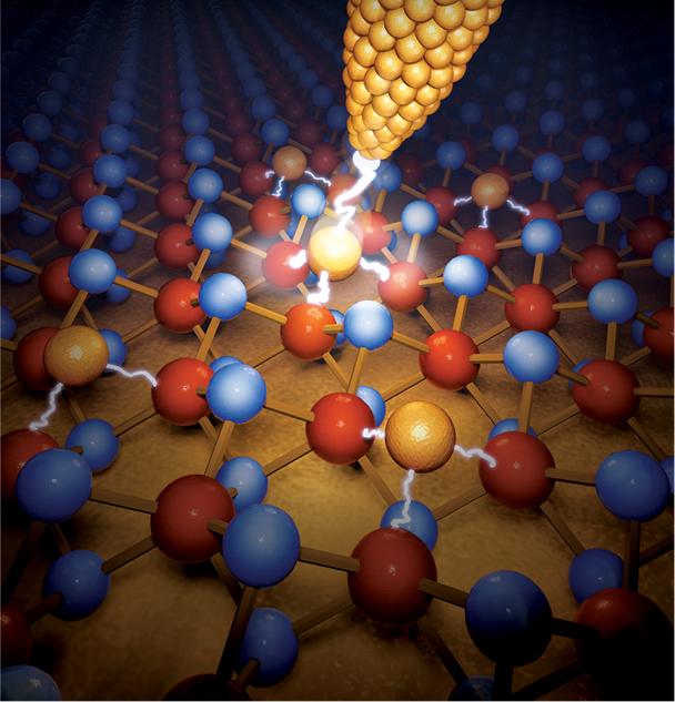
- Shaochuan Chen, Mohammad Reza Mahmoodi, Yuanyuan Shi, Chandreswar Mahata, Bin Yuan, Xianhu Liang, Chao Wen, Fei Hui, Deji Akinwande, Dmitri B. Strukov & Mario Lanza
“Wafer-scale integration of two-dimensional materials in high-density memristive crossbar arrays for artificial neural networks”; Nature Electronics, October 2020;.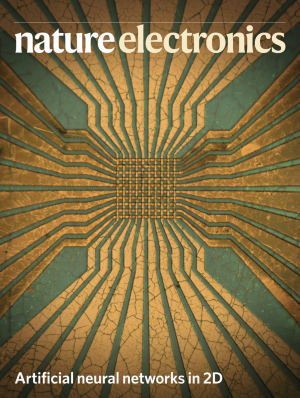
- Nathan C. Frey, Deji Akinwande, Deep Jariwala, Vivek B. Shenoy
“Machine Learning-Enabled Design of Point Defects in 2D Materials for Quantum and Neuromorphic Information Processing”; ACS Nano, September 2020;.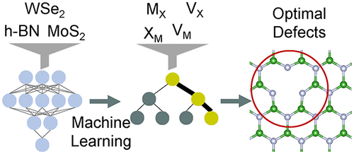
- Christian Martella, Gabriele Faraone, Muhammad Hasibul Alam, Deepyanti Taneja, Li Tao, Guido Scavia, Emiliano Bonera, Carlo Grazianetti, Deji Akinwande, Alessandro Molle
“Disassembling Silicene from Native Substrate and Transferring onto an Arbitrary Target Substrate”; Advanced Functional Materials, August 2020;.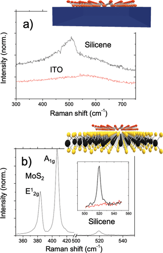
- Miss Wen Zhong, Dr Yu Zhao, Dr Beibei Zhu, Dr Jingjie Sha, Dr Emily S. Walker, Dr Seth R Bank, Professor Yunfei Chen, Professor Deji Akinwande and Dr Li Tao
“Anisotropic thermoelectric effect and field-effect devices in epitaxial bismuthene on Si (111)”; Nanotechnology, August 2020;.
- Mamoon Asghar, Syedah Afsheen Zahra, Zarah Khan, Momina Ahmed, Farheen Nasir, Mudassir Iqbal, Mohammad Ali Mohammad, Asif Mahmood, Deji Akinwande, Syed Rizwan
“Laser-Assisted Fabrication of Nanostructured Substrate Supported Electrodes for Highly Active Supercapacitors “; Energy Materials, July 2020;.
- Xiaohan Wu, Ruijing Ge, Deji Akinwande and Jack C. Lee
“Understanding of Multiple Resistance States by Current Sweeping in MoS2-based Non-volatile Memory Devices”; Nanotechnology, July 2020;.
- Yury Yu. Illarionov, Theresia Knobloch, Markus Jech, Mario Lanza, Deji Akinwande, Mikhail I. Vexler, Thomas Mueller, Max C. Lemme, Gianluca Fiori, Frank Schwierz & Tibor Grasser
“Insulators for 2D nanoelectronics: the gap to bridge”; Nature Communications, July 2020;.PDF Copy.
- Oluwadamilola Oshin, Dmitry Kireev, Hanna Hlukhova, Francis Idachaba, Deji Akinwande and Aderemi Atayero
“Graphene-Based Biosensor for Early Detection of Iron Deficiency”; Sensors, July 2020;.PDF Copy.
- Md Hasibul Alam, Zifan Xu, Sayema Chowdhury, Zhanzhi Jiang, Deepyanti Taneja, Sanjay K. Banerjee, Keji Lai, Maria Helena Braga, Deji Akinwande
“Lithium-ion electrolytic substrates for sub-1V high-performance transition metal dichalcogenide transistors and amplifiers”; Nature Communication, June 2020;.PDF Copy.
- Myungsoo Kim, Emiliano Pallecchi, Ruijing Ge, Xiaohan Wu, Guillaume Ducournau, Jack C. Lee, Henri Happy and Deji Akinwande,
“Analog switches made from boron nitride monolayers for application in 5G and terahertz communication systems”; Nature Electronics, May 2020;.PDF Copy.
- Jameela Fatheema, Tauseef Shahid, Mohammad Ali Mohammad, Amjad Islam, Fouzia Malik, Deji Akinwande and Syed Rizwan,
“A comprehensive investigation of MoO3 based resistive random access memory”; RSC Advances, May 2020;.
- Zaheer Ud Din Babar, Shahbaz Anwar, Muhammad Mumtaz, Mudassir Iqbal, Ren-Kui Zheng, Deji Akinwande and Syed Rizwan,
“Peculiar Magnetic Behaviour and Meissner Effect in Two-dimensional Layered Nb2C MXene”; 2D Materials, April 2020;. - Sunaina Rafiq, SaifUllah Awan, Ren-Kui Zheng, Zhenchao Wen, Malika Rani, Deji Akinwande, Syed Rizwan,
“Novel room-temperature ferromagnetism in Gd-doped 2-dimensional Ti3C2Tx MXene semiconductor for spintronics”; Journal of Magnetism and Magnetic Materials, March 2020;. - Mahjabeen Fatima, Jameela Fatheema, Nasbah B Monir, Ahmad Hassan Siddiqui, Bushra Khan, Amjad Islam, Deji Akinwande, Syed Rizwan,
“Nb-doped Two-dimensional MXene with Enhanced Energy Storage Capacity and Stability”; Front. Chem., 03 April 2020;.

2019
- Deji Akinwande, Cedric Huyghebaert, Ching-Hua Wang, Martha I. Serna, Stijn Goossens, Lain-Jong Li, H.-S. Philip Wong and Frank H. L. Koppens,
“Graphene and two-dimensional materials for silicon technology”; Nature, Sep. 2019;.PDF Copy.
- Weiyi Lin, Pingping Zhuang, Deji Akinwande, Xue-Ao Zhang, and Weiwei Cai,
“Oxygen-assisted synthesis of hBN films for resistive random access memories”; Appl. Phys. Lett., July 2019;.PDF Copy.
- Emily S. Walker, Sarah Muschinske, Christopher J. Brennan, Seung Ryul Na, Tanuj Trivedi, Stephen D. March, Yukun Sun, Tianhao Yang, Alice Yau, Daehwan Jung, Andrew F. Briggs, Erica M. Krivoy, Minjoo L. Lee, Kenneth M. Liechti, Edward T. Yu, Deji Akinwande, and Seth R. Bank,
“Composition-dependent structural transition in epitaxial
Bi1-xSbx thin films on Si(111)”; Phys. Rev. Materials, Jun. 2019;.PDF Copy.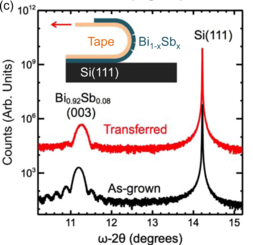
- Xu Jing, Francesco Maria Puglisi, Deji Akinwande and Mario Lanza,
“Chemical vapor deposition of hexagonal boron nitride on metal-coated wafers and transfer-free fabrication of resistive switching devices”; 2D Materials, Apr. 2019;.PDF Copy.
- Maciej Wiesner, Richard H. Roberts, Jung-Fu. Lin, Deji Akinwande, Thorsten Hesjedal, Liam B. Duffy, Shumin Wang, Yuxin Song, Jacek Jenczyk, Stefan Jurga and Boguslaw Mroz,
“The effect of substrate and surface plasmons on symmetry breaking at the substrate interface of the topological insulator Bi2Te3”; Scientific Reports, Apr. 2019;.PDF Copy.
- Weiyi Lin, Pingping Zhuang, Harry Chou, Yuqian Gu, Richard Roberts, Wei Li, Sanjay K. Banerjee, Weiwei Cai, and Deji Akinwande,
“Electron redistribution and energy transfer in graphene/MoS2 heterostructure”; Appl. Phys. Lett., Mar. 2019;.PDF Copy.
- Di Wu, Wei Li, Amritesh Rai, Xiaoyu Wu, Hema C. P. Movva, Maruthi N. Yogeesh, Zhaodong Chu, Sanjay K. Banerjee, Deji Akinwande, Keji Lai
“Visualization of Local Conductance in MoS2/WSe2 Heterostructure Transistors”; Nano Lett., Feb. 2019;.PDF Copy.
- Xiaohan Wu*, Ruijing Ge*, Po‐An Chen, Harry Chou, Zhepeng Zhang, Yanfeng Zhang, Sanjay Banerjee, Meng‐Hsueh Chiang, Jack C. Lee and Deji Akinwande,
“Thinnest Nonvolatile Memory Based on Monolayer h‐BN”; Advanced Materials, Feb. 2019; * equal contribution.PDF Copy.
2018
- Weinan Zhu, Liangbo Liang, Richard H. Roberts, Jung-Fu Lin, and Deji Akinwande,
“Anisotropic Electron–Phonon Interactions in Angle-Resolved Raman Study of Strained Black Phosphorus”; ACS Nano, Dec. 2018; PDF Copy.
- Shijiao Han, Zuchong Yang, Zongkang Li, Xinming Zhuang, Deji Akinwande, and Junsheng Yu,
“Improved Room Temperature NO2 Sensing Performance of Organic Field-Effect Transistor by Directly Blending a Hole-Transporting/Electron-Blocking Polymer into the Active Layer”; ACS Appl. Mater. Interfaces, Oct. 2018; PDF Copy.
- Ayesha Tariq, S. Irfan Ali, Deji Akinwande, and Syed Rizwan,
“Efficient Visible-Light Photocatalysis of 2D-MXene Nanohybrids with Gd3+– and Sn4+-Codoped Bismuth Ferrite”; ACS Omega, Oct. 2018; PDF Copy.
- Mario Lanza, H.-S. Philip Wong, Eric Pop, Daniele Ielmini, Dimitri Strukov, Brian C. Regan, Luca Larcher, Marco A. Villena, J. Joshua Yang, Ludovic Goux, Attilio Belmonte, Yuchao Yang, Francesco M. Puglisi, Jinfeng Kang, Blanka Magyari-Köpe, Eilam Yalon, Anthony Kenyon, Mark Buckwell, Adnan Mehonic, Alexander Shluger, Haitong Li, Tuo-Hung Hou, Boris Hudec, Deji Akinwande, Ruijing Ge, Stefano Ambrogio, Juan B. Roldan, Enrique Miranda, Jordi Suñe, Kin Leong Pey, Xing Wu, Nagarajan Raghavan, Ernest Wu, Wei D. Lu, Gabriele Navarro, Weidong Zhang, Huaqiang Wu, Runwei Li, Alexander Holleitner, Ursula Wurstbauer, Max C. Lemme, Ming Liu, Shibing Long, Qi Liu, Hangbing Lv, Andrea Padovani, Paolo Pavan, Ilia Valov, Xu Jing, Tingting Han, Kaichen Zhu, Shaochuan Chen, Fei Hui, and Yuanyuan Shi,
“Recommended Methods to Study Resistive Switching Devices”; Advanced Electronic Materials, Sep. 2018; PDF Copy.
- Sabeen Fatima, S. Irfan Ali, Daniyal Younas, Amjad Islam, Deji Akinwande and Syed Rizwan,
“Graphene nanohybrids for enhanced catalytic activity and large surface area”; MRS Commun., Sep. 2018; PDF Copy.
- Linhan Lin*, Jingang Li*, Wei Li*, Maruthi N. Yogeesh, Jianjian Shi, Xiaolei Peng, Yaoran Liu, Bharath Bangalore Rajeeva, Michael F. Becker, Yuanyue Liu, Deji Akinwande, Yuebing Zheng,
“Optothermoplasmonic Nanolithography for On-Demand Patterning of 2D Materials”; Adv. Funct. Mater., Aug. 2018,* equal contribution; PDF Copy.
- Alessandro Molle, Carlo Grazianetti, Li Tao, Deepyanti Taneja, Md. Hasibul Alam and Deji Akinwande,
“Silicene, silicene derivatives, and their device applications”; Chemical Society Reviews, Aug. 2018; PDF Copy.
- Zuchong Yang, Shijiao Han, Yufan Liu, Xinming Zhuang, Deji Akinwande, Junsheng Yu,
“Investigation of the atmosphere influence on device characteristics and NO2 sensing performance of organic field-effect transistors consisting of polymer bulk heterojunction”; Organic Electronics, July 2018; PDF Copy.
- Shideh Kabiri Ameri, Myungsoo Kim, Irene Agnes Kuang, Withanage K. Perera, Mohammed Alshiekh, Hyoyoung Jeong, Ufuk Topcu, Deji Akinwande, Nanshu Lu,
“Imperceptible electrooculography graphene sensor system for human–robot interface”; npj 2D Materials and Applications, July 2018; PDF Copy.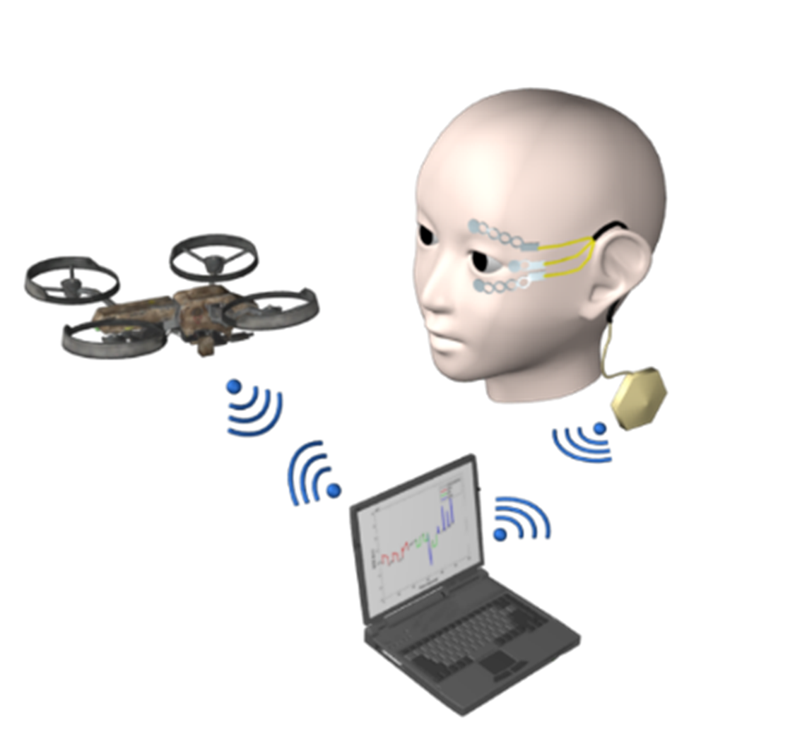
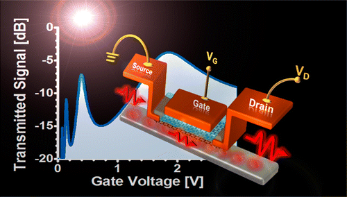
- Myungsoo Kim*, Ruijing Ge*, Xiaohan Wu*, Xing Lan, Jesse Tice, Jack C. Lee, Deji Akinwande,
“Zero-static power radio-frequency switches based on MoS2 atomristors”; Nature Communications, June 2018 (Editors Choice); * equal contribution; PDF Copy.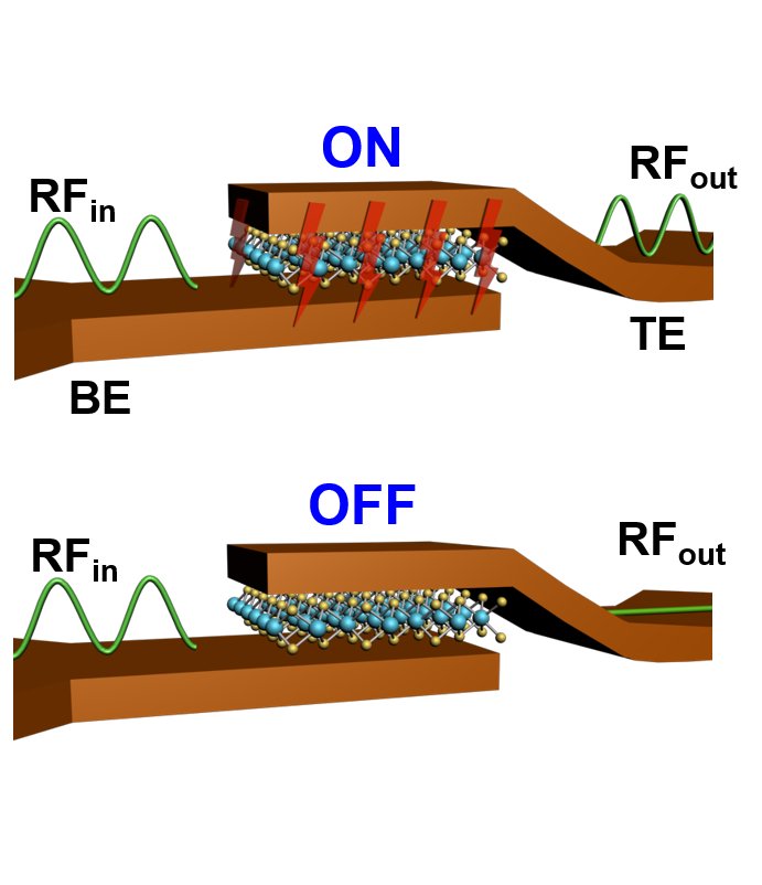
- Yohannes Abate, Deji Akinwande, Sampath Gamage, Han Wang, Michael Snure, Nirakar Poudel, Stephen B. Cronin,
“Recent Progress on Stability and Passivation of Black Phosphorus”; Advanced Materials, May 2018; PDF Copy.
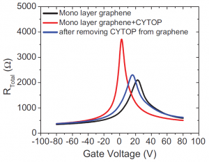
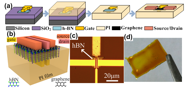
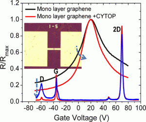
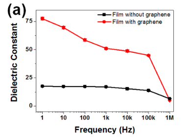
- Saungeun Park, Hsiao‐Yu Chang, Somayyeh Rahimi, Alvin L. Lee, Li Tao, Deji Akinwande,
“Transparent Nanoscale Polyimide Gate Dielectric for Highly Flexible Electronics”; Advanced Electronic Materials, Jan. 2018;
- David Choi, Nirakar Poudel, Saungeun Park, Deji Akinwande, Stephen B. Cronin, Kenji Watanabe, Takashi Taniguchi, Zhen Yao, and Li Shi,
“Large Reduction of Hot Spot Temperature in Graphene Electronic Devices with Heat-Spreading Hexagonal Boron Nitride”; ACS Appl. Mater. Interfaces, Mar. 2018; PDF Copy.
- Joon-Seok Kim, Rinkle Juneja, Nilesh P. Salke, Witold Palosz, Venkataraman Swaminathan, Sudhir Trivedi, Abhishek K. Singh, Deji Akinwande, and Jung-Fu Lin,
“Structural, vibrational, and electronic topological transitions of Bi1.5Sb0.5Te1.8Se1.2 under pressure”; Journal of Applied Physics, Mar. 2018;PDF Copy.
- Ruijing Ge*, Xiaohan Wu*, Myungsoo Kim, Jianping Shi, Sushant Sonde, Li Tao, Yanfeng Zhang, Jack C. Lee, and Deji Akinwande,
“Atomristor: Nonvolatile Resistance Switching in Atomic Sheets of Transition Metal Dichalcogenides”; Nanoletters, Jan. 2018 (Editors Choice); * equal contribution. PDF Copy.
2017
- Seyedeh Maryam Mortazavi Zanjani, Milo Holt, Mir Mohammad Sadeghi, Somayyeh Rahimi & Deji Akinwande
“3D integrated monolayer graphene–Si CMOS RF gas sensor platform”; npj 2D Materials and Applications, Oct 2017;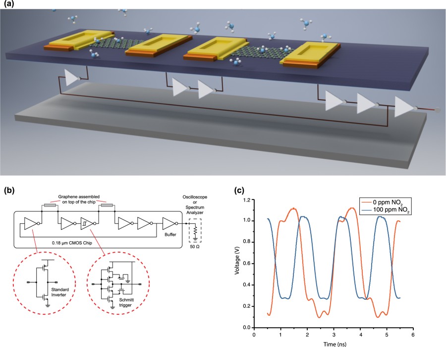
- Weinan Zhu, Saungeun Park, Maruthi N Yogeesh and Deji Akinwande
“Advancements in 2D flexible nanoelectronics: from material perspectives to RF applications”; Flexible and Printed Electronics, Oct 2017;
- Joon-Seok Kim, Rafia Ahmad, Tribhuwan Pandey, Amritesh Rai, Simin Feng, Jing Yang, Zhong Lin, Mauricio Terrones, Sanjay K Banerjee, Abhishek K Singh, Deji Akinwande, and Jung-Fu Lin
“Towards band structure and band offset engineering of monolayer Mo(1−x)W(x)S2 via Strain”; 2D Materials, Oct 2017;
- Mingsong Wang, Wei Li, Leonardo Scarabelli, Bharath Bangalore Rajeeva, Mauricio Terrones, Luis M. Liz-Marzán, Deji Akinwande and Yuebing Zheng
“Plasmon–trion and plasmon–exciton resonance energy transfer from a single plasmonic nanoparticle to monolayer MoS2”; Nanoscale, Sep. 2017; - Atresh Sanne, Saungeun Park, Rudresh Ghosh, Maruthi Nagavalli Yogeesh, Chison Liu, Leo Mathew, Rajesh Rao, Deji Akinwande and Sanjay Kumar Banerjee
“Embedded gate CVD MoS2 microwave FETs”; Nature 2D Materials and Applications, Aug. 2017;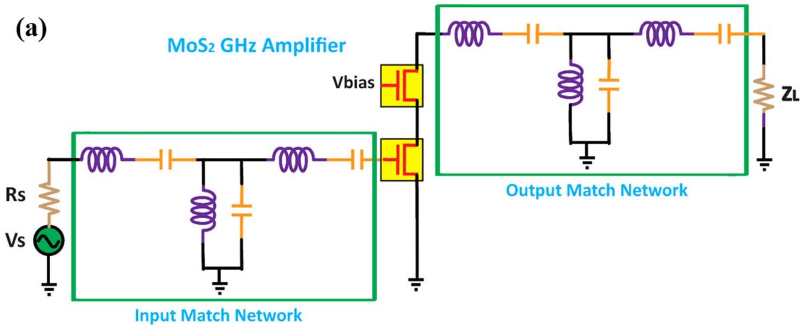
- Shideh Kabiri Ameri, Rebecca Ho, Hongwoo Jang, Li Tao, Youhua Wang, Liu Wang, David M. Schnyer, Deji Akinwande, and Nanshu Lu
“Graphene Electronic Tattoo Sensors”; ACS Nano, July, 2017; (PDF)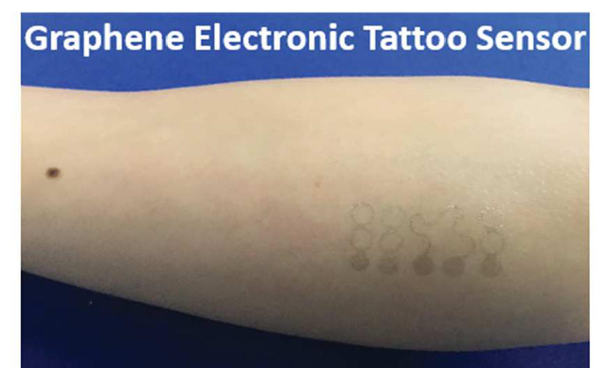
- Yu. Yu. Illarionov, M. Waltl, G. Rzepa, T. Knobloch, J.-S. Kim, D. Akinwande, T. Grasser
“Highly-stable black phosphorus field-effect transistors with low density of oxide traps”; Nature 2D Materials and Applications, July, 2017;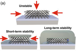
- Ke Chen, Rudresh Ghosh, Xianghai Meng, Anupam Roy, Joon-Seok Kim, Feng He, Sarah C. Mason, Xiaochuan Xu, Jung-Fu Lin, Deji Akinwande, Sanjay K. Banerjee & Yaguo Wang;
“Experimental evidence of exciton capture by mid-gap defects in CVD grown monolayer MoSe2”; Nature 2D Materials and Applications, June, 2017;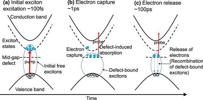
- Carlo Grazianetti, Eugenio Cinquanta, Li Tao, Paola De Padova, Claudio Quaresima, Carlo Ottaviani, Deji Akinwande, and Alessandro Molle;
“Silicon Nanosheets: Crossover between Multilayer Silicene and Diamond-like Growth Regime”; ACS Nano, March, 2017;
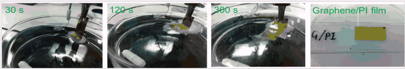
- Xiaohan Wang, Andrei Dolocan, Harry Chou, Li Tao, Andrew Dick, Deji Akinwande, and C. Grant Willson;
“Direct Observation of Poly(Methyl Methacrylate) Removal from a Graphene Surface”; Chem. Mater., January, 2017;
- Deji Akinwande, Christopher J. Brennan, J. Scott Bunch, Philip Egberts, Jonathan R. Felts, Huajian Gao, Rui Huang, Joon-Seok Kim, Teng Li, Yao Li, Kenneth M. Liechti, Nanshu Lu, Harold S. Park, Evan J. Reed, Peng Wang, Boris I. Yakobson, Teng Zhang, Yong-Wei Zhang, Yao Zhou, Yong Zhu;
“A review on mechanics and mechanical properties of 2D materials—Graphene and beyond”; Extreme Mechanics Letters, Jan. 2017;
- Wonbong Choi, Nitin Choudhary, Gang Hee Han, Juhong Park, Deji Akinwande, Young Hee Lee;
“Recent development of two-dimensional transition metal dichalcogenides and their applications”; Materials Today, Jan. 2017;
- Alessandro Molle, Joshua Goldberger, Michel Houssa, Yong Xu, Shou-Cheng Zhang and Deji Akinwande;
“Buckled two-dimensional Xene sheets”; Nature Materials, Jan. 2017;
2016
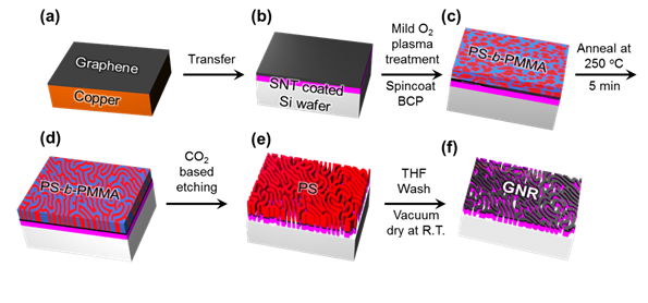
- Reika Katsumata, Maruthi Nagavalli Yogeesh, Helen Wong, Sunshine X.Zhou, Stephen M. Sirard, Tao Huang, Richard D. Piner, Zilong Wu, Wei Li, Alvin L. Lee, Matthew Carlson, Michael Maher, Deji Akinwande, Christopher J. Ellison; “Large area fabrication of graphene nanoribbons by wetting transparency-assisted block copolymer lithography”; Polymer, Dec 2016;
- Pengchao Lu,* Joon-Seok Kim,* Jing Yang, Hao Gao, Juefei Wu, Dexi Shao, Bin Li, Da Wei Zhou, Jian Sun, Deji Akinwande, Jung-Fu Lin, Dingyu Xing; “Origin of the Superconductivity of Weyl Semimetal WTe2 under Pressure”; Physical Review B, Dec 2016; * equal contribution
-
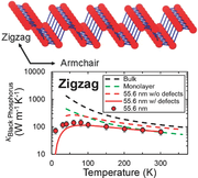
Brandon Smith, Bjorn Vermeersch, Jesús Carrete, Eric Ou, Jaehyun Kim, Natalio Mingo, Deji Akinwande, Li Shi; “Temperature and Thickness Dependences of the Anisotropic In-Plane Thermal Conductivity of Black Phosphorus”; Advanced Materials, 24 November 2016;
-
Emily S. Walker, Seung Ryul Na, Daehwan Jung, Stephen D. March, Joon-Seok Kim, Tanuj Trivedi, Wei Li, Li Tao, Minjoo L. Lee, Kenneth M. Liechti, Deji Akinwande, and Seth R. Bank; “Large-Area Dry Transfer of Single-Crystalline Epitaxial Bismuth Thin Films”; Nano Lett., 19 Oct. 2016;

-
Yury Yuryevich Illarionov, Michael Waltl, Gerhard Rzepa, Joon-Seok Kim, Seohee Kim, Ananth Dodabalapur, Deji Akinwande, and Tibor Grasser; “Long-Term Stability and Reliability of Black Phosphorus Field-Effect Transistors”; ACS Nano, Oct. 5, 2016;

-
Zilong Wu, Glen Kelp, Maruthi Nagavalli Yogeesh, Wei Li, Kyle M. McNicholas, Andrew Frederick Briggs, Bharath Bangalore Rajeeva, Deji Akinwande, Seth R. Bank, Gennady Shvets and Yuebing Zheng; ” Dual-Band Moiré Metasurface Patches for Multifunctional Biomedical Applications” Nanoscale, 2016, Highlighted by Nanowerk;
-
Somayyeh Rahimi, Rudresh Ghosh, Seohee Kim, Ananth Dodabalapur, Sanjay Banerjee and Deji Akinwande; “The Positive Effects of Hydrophobic Fluoropolymers on the Electrical Properties of MoS2 Transistors”; Appl. Sci., 19 July 2016;
-
Zilong Wu, Wei Li, Maruthi Nagavalli Yogeesh, Seungyong Jung, Alvin Lynghi Lee, Kyle McNichola, Andrew Briggs, Seth Bank, Mikhail Belkin, Deji Akinwande*, and Yuebing Zheng*; “Tunable and Gradient Graphene Metasurfaces by Self-assembly-based Moiré Nanosphere Lithography”; Advanced Optical Materials, 11 August 2016; Highlighted by Nanowerk; Nanotechweb;
This paper has been featured as an inside cover of Advanced Optical Materials. (Dec 2016 issue)
-
Di Wu, Xiao Li, Lan Luan, Xiaoyu Wu, Wei Li, Maruthi N. Yogeesh, Rudresh Ghosh, Zhaodong Chu,Deji Akinwande, Qian Niu, and Keji Lai; “Uncovering edge states and electrical inhomogeneity in MoS2 field-effect transistors”; PNAS, 20 June 2016; Highlighted by PHYS.ORG; AZONANO; Science Daily
-
Tribhuwan Pandey, Avinash P. Nayak, Jin Liu, Samuel T. Moran, Joon-Seok Kim, Lain-Jong Li, Jung-Fu Lin, Deji Akinwande, Abhishek K. Singh; “Pressure-Induced Charge Transfer Doping of Monolayer Graphene/MoS2 Heterostructure”; Small, 20 June 2016;
-
Mir Mohammad Sadeghi, Saungeun Park, Yu Huang, Deji Akinwande, Zhen Yao, Jayathi Murthy and Li Shi; “Quantitative scanning thermal microscopy of graphene devices on flexible polyimide substrates”;J. Appl. Phys. 119, 235101 (2016);
-
Ke Chen, Maruthi Nagavalli Yogeesh, Yuan Huang, Shaoqing Zhang, Feng He, Xianghai Meng,Shaoyin Fang, Nathanial Sheehan, Tiger Hu Tao, Seth R. Bank, Jung-Fu Lin, Deji Akinwande, Peter Sutter, Tianshu Lai, Yaguo Wang,
; “Non-destructive measurement of photoexcited carrier transport in graphene with ultrafast grating imaging technique”;Carbon, June 2016;
-
Haiyu Huang, Li Tao, Fei Liu, Li Ji, Ye Hu, Mark Ming-Cheng Cheng, Pai-Yen Chen & Deji Akinwande; “Chemical-sensitive graphene modulator with a memory effect for internet-of-things applications”;Nature. Microsystems & Nanoengineering, 09 May 2016;
-
Haiyu Huang, Maryam Sakhdari, Mehdi Hajizadegan, Ali Shahini, Deji Akinwande, Pai-Yen Chen; “Toward transparent and self-activated graphene harmonic transponder sensors”;Applied Physics Letters, April 25, 2016;
-
S. R. Na, S. Rahimi, L. Tao, H. Chou, S. K. Ameri, D. Akinwande and K. M. Liechti; “Clean graphene interfaces by selective dry transfer for large area silicon integration”;Nanoscale, 05 Feb 2016;
-
Joon-Seok Kim, Samuel T Moran, Avinash P Nayak, Shahar Pedahzur, Itzel Ruiz, Gabriela Ponce, Daniela Rodriguez, Joanna Henny, Jin Liu, Jung-Fu Lin and Deji Akinwande; “High pressure Raman study of layered Mo0.5W0.5S2 ternary compound”;30 March 2016, IOP Publishing Ltd;

-
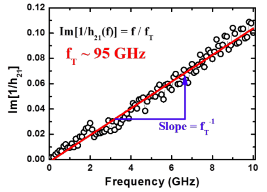
Weinan Zhu, Saungeun Park, Maruthi N. Yogeesh, Kyle M. McNicholas, Seth R. Bank, and Deji Akinwande; “Black Phosphorus Flexible Thin Film Transistors at Gighertz Frequencies”;Nano Lett. Mar. 2016;
-
Saungeun Park, Seung Heon Shin, Maruthi N. Yogeesh, Alvin L. Lee, Somayyeh Rahimi, and Deji Akinwande; “Extremely High Frequency Flexible Graphene Thin Film Transistors”;IEEE Electron Device Letters Feb. 2016;
-
Sk. F. Chowdhury*, Maruthi N. Yogeesh*, Sanjay K. Banerjee, Fellow, IEEE, and Deji Akinwande; “Black Phosphorous Thin-film Transistor and RF Circuit Applications”;IEEE Electron Device Letters, Feb. 2016; * equal contribution
-
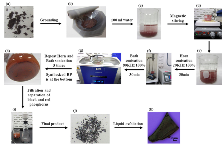
Sandra H Aldave, Maruthi N Yogeesh, Weinan Zhu, Joonseok Kim, Sushant S Sonde, Avinash P Nayak and Deji Akinwande; “Characterization and sonochemical synthesis of black phosphorus from red phosphorus”;2D Mater. 3 (2016);
-
Haiyu Huang, Pai-Yen Chen, Cheng-Hsien Hung, Ranjit Gharpurey & Deji Akinwande; “A zero power harmonic transponder sensor for ubiquitous wireless μL liquid-volume monitoring”;Scientific Reports 6, Article number: 18795 (2016);
-
Rudresh Ghosh, Joon-Seok Kim, Anupam Roy, Harry Chou, Mary Vu, Sanjay K. Banerjee and Deji Akinwande; “Large area chemical vapor deposition growth of monolayer MoSe2 and its controlled sulfurization to MoS2”;Journal of Materials Research, 2016;
-
Seyedeh Maryam Mortazavi Zanjani, Mir Mohammad Sadeghi, Milo Holt, Sk. Fahad Chowdhury, Li Tao and Deji Akinwande; “Enhanced sensitivity of graphene ammonia gas sensors using molecular doping”;Appl. Phys. Lett. 108, 033106 (2016);
2015
-
Bin Wang, Ming Huang, Li Tao, Sun Hwa Lee, A-Rang Jang, Bao-Wen Li, Hyeon Suk Shin, Deji Akinwande, and Rodney S. Ruoff; “Support-Free Transfer of Ultrasmooth Graphene Films Facilitated by Self-Assembled Monolayers for Electronic Devices and Patterns”;ACS Nano, Dec 2015;
-
Hsiao-Yu Chang*, Maruthi Nagavalli Yogeesh*, Rudresh Ghosh, Amritesh Rai, Atresh Sanne, Shixuan Yang, Nanshu Lu, Sanjay Kumar Banerjee, Deji Akinwande; “Large-area monolayer MoS2 for flexible low-power RF nanoelectronics in the GHz regime”;Advanced Materials Dec 2015; *equal contribution
-
Linhan Lin, Xiaolei Peng, Zhangming Mao, Wei Li, Maruthi N. Yogeesh, Bharath Bangalore Rajeeva, Evan P. Perillo, Andrew K. Dunn, Deji Akinwande, and Yuebing Zheng; “Bubble-Pen Lithography,”;Nano Letters Dec 2015
-
M. Yogeesh, K. N. Parrish, J. Lee, S. Park, L. Tao, and D. Akinwande; “Towards the Realization of Graphene Based Flexible Radio Frequency Receiver,”;Electronics, vol. 4, p. 933, 2015
-
G. R. Bhimanapati, Z. Lin, V. Meunier, Y. Jung, J. J. Cha, S. Das, D. Xiao, Y. Son, M. S. Strano, V. R. Cooper, L. Liang, S. G. Louie, E. Ringe, W. Zhou, B. G. Sumpter, H. Terrones, F. Xia, Y. Wang, J. Zhu, D. Akinwande, N. Alem, J. A. Schuller, R. E. Schaak, M. Terrones, and J. A. Robinson; “Recent Advances in Two-Dimensional Materials Beyond Graphene,”;ACS Nano, Nov. 2015
-
A. P. Nayak, T. Pandey, D. Voiry, J. Liu, S. T. Moran, A. Sharma, C. Tan, C.-H. Chen, L.-J. Li, M. Chhowalla, J.-F. Lin, A. Singh, and D. Akinwande; “Pressure-Dependent Optical and Vibrational Properties of Monolayer Molybdenum Disulfide,”;Nano Letters, vol. 15, 2015.
-
Y. Liu, C. Tan, H. Chou, A. Nayak, D. Wu, R. Ghosh, H.-Y. Chang, Y. Hao, X. Wang, J.-S. Kim, R. Piner, R. S. Ruoff, D. Akinwande, and K. Lai; “Thermal Oxidation of WSe2 Nanosheets Adhered on SiO2/Si Substrates,”;Nano Lett., 2015, 15 (8), pp 4979–4984
-
A. P. Nayak, Z. Yuan, B. Cao, J. Liu, J. Wu, S. T. Moran, T. Li, D. Akinwande, C. Jin, and J.-F. Lin; “Pressure-Modulated Conductivity, Carrier Density, and Mobility of Multilayered Tungsten Disulfide,”;ACS Nano, 2015, 9 (9), pp 9117–9123.
-
W. Kim, C. Li, N. Chekurov, S. Arpiainen, D. Akinwande, H. Lipsanen, and J. Riikonen; “All-Graphene Three-Terminal-Junction Field-Effect Devices as Rectifiers and Inverters,”;ACS Nano, 2015, 9 (6), pp 5666–5674
-
B. C. Worley, S. Kim, S. Park, P. J. Rossky, D. Akinwande, and A. Dodabalapur; “Dramatic vapor-phase modulation of the characteristics of graphene field-effect transistors,”;Phys. Chem. Chem. Phys., 2015,17, 18426-18430
-
Z. Cao, L. Tao, D. Akinwande, R. Huang, and K. M. Liechti; “Mixed-Mode Interactions between Graphene and Substrates by Blister Tests,”;Journal of Applied Mechanics, 2015..
-
D. Akinwande, L. Tao, Q. Yu, X. Lou, P. Peng, and D. Kuzum; “Large-Area Graphene Electrodes: Using CVD to facilitate applications in commercial touchscreens, flexible nanoelectronics, and neural interfaces,”;Nanotechnology Magazine, IEEE, vol. 9, pp. 6-14, 2015.
-
Atresh Sanne, Rudresh Ghosh, Amritesh Rai, Maruthi Nagavalli Yogeesh, Seung Heon Shin, Ankit Sharma, Karalee Jarvis, Leo Mathew, Rajesh Rao, Deji Akinwande, and Sanjay K. Banerjee; “Radio Frequency Transistors and Circuits Based on CVD MoS2”;Nano Letters, July 2015.
-
Joon-Seok Kim, Yingnan Liu, Weinan Zhu, Seohee Kim, Di Wu, Li Tao, Ananth Dodabalapur, Keji Lai & Deji Akinwande; “Toward air-stable multilayer phosphorene thin-films and transistors”;SCIENTIFIC REPORTS, March 2015.
-
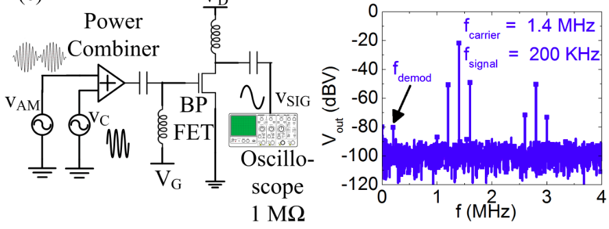
Weinan Zhu, Maruthi N. Yogeesh, Shixuan Yang, Sandra H. Aldave, Joon-Seok Kim, Sushant Sonde , Li Tao, Nanshu Lu, and Deji Akinwande; “Flexible Black Phosphorus Ambipolar Transistors, Circuits and AM Demodulator”;Nano Letters, Febraury 2015.
-
Li Tao, Eugenio Cinquanta, Daniele Chiappe, Carlo Grazianetti, Marco Fanciulli, Madan Dubey, Alessandro Molle & Deji Akinwande; “Silicene field-effect transistors operating at room temperature”;Nature Nanotechnology, Feb 2015.
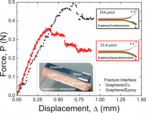
- Seung Ryul Na, Ji Won Suk, Li Tao, Deji Akinwande, Rodney S. Ruoff, Rui Huang, and Kenneth M. Liechti; “Selective Mechanical Transfer of Graphene from Seed Copper Foil Using Rate Effects” ACS Nano, Feb 2015.
2014
- Deji Akinwande, Nicholas Petrone and James Hone; “Two-dimensional flexible nanoelectronics“; Nature Communications, Oct 2014.

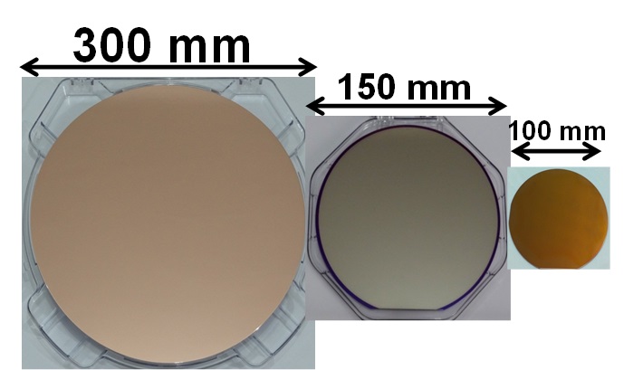
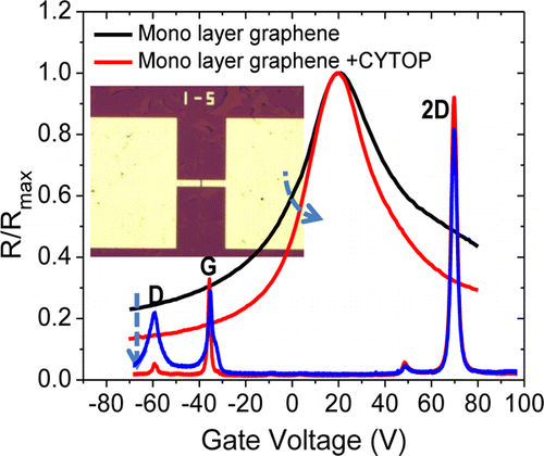
- S. Rahimi, L. Tao, S. F. Chowdhury, S. Park, A. Jouvray, S. Buttress, N. Rupesinghe, K. Teo, and D. Akinwande, “Toward 300 mm Wafer-Scalable High-Performance Polycrystalline Chemical Vapor Deposited Graphene Transistors,” ACS Nano, 2014.
- S. F. Chowdhury, S. Sonde, S. Rahimi, L. Tao, S. Banerjee, and D. Akinwande, “Improvement of graphene field-effect transistors by hexamethyldisilazane surface treatment,” Applied Physics Letters, vol. 105, pp. -, 2014.
- P.-Y. Chen, H. Huang, D. Akinwande, and A. Alù, “Graphene-Based Plasmonic Platform for Reconfigurable Terahertz Nanodevices,” ACS Photonics, 2014.
- Avinash P. Nayak, Swastibrata Bhattacharyya, Jie Zhu, Jin Liu, Xiang Wu, Tribhuwan Pandey, Changqing Jin, Abhishek K. Singh, Deji Akinwande & Jung-Fu Lin; “Pressure-induced semiconducting to metallic transition in multilayered Molybdenum disulphide” Nature Communications, May 2014.
- Z. Cao, P. Wang, W. Gao, L. Tao, J.W. Suk, R.S. Ruoff, D. Akinwande, R. Huang, K.M. Liechti, “ A BLISTER TEST FOR INTERFACIAL ADHESION OF LARGE-SCALE TRANSFERRED GRAPHENE” CARBON Vol69, April 2014
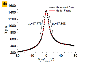
- Hsiao-Yu Chang, Weinan Zhu1 and Deji Akinwande; “On the mobility and contact resistance evaluation for transistors based on MoS2 or two-dimensional semiconducting atomic crystals” APL March 2014

- Haiyu Huang, Peisen Zhao, Pai-Yen Chen, Yong Ren, Mauro Ferrari, Deji Akinwande; “RFID Tag Helix Antenna Sensors for Wireless Drug Dosage Monitoring” IEEE Journal in Translational Engineering in Health and Medical Sciences, March 2014.


2013
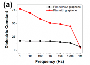
- Jin-Young Kim, Jongho Lee,Wi Hyoung Lee, Iskandar N. Kholmanov, Ji Won Suk , TaeYoung Kim, Yufeng Hao, Harry Chou, Deji Akinwande , and Rodney S. Ruoff ; “Flexible and Transparent Dielectric Film with a High Dielectric Constant Using Chemical Vapor Deposition-Grown Graphene Interlayer” ACS Nano Dec 2013 (pdf)
- Li Tao, Jongho Lee, Huifeng Li, Richard D. Piner, Rodney S. Ruoffand Deji Akinwande, “Inductively heated synthesized graphene with record transistor mobility on oxidized silicon substrates at room temperature” APL, November 2013 (pdf)
- AVINASH P. NAYAK, ANDREI DOLOCAN, JONGHO LEE, HSIAO-YU CHANG, TWINKLE PANDHI, MILO HOLT, LI TAO, and DEJI AKINWANDE, “INVERSION OF THE ELECTRICAL AND OPTICAL PROPERTIES OF PARTIALLY OXIDIZED HEXAGONAL BORON NITRIDE” Nano, World Scientific, October 2013 (pdf)
- Xiaohan Wang, Li Tao, Yufeng Hao, Zhihong Liu, Harry Chou, Iskandar Kholmanov, Shanshan Chen, Cheng Tan, Nishant Jayant, Qingkai Yu, Deji Akinwande, Rodney S. Ruoff, ” Direct Delamination of Graphene for High-Performance Plastic Electronics” Small, Wiley Online Library, September 2013 (pdf)
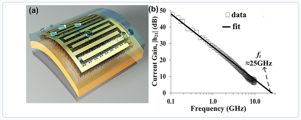
- Jongho Lee, Tae-Jun Ha, Huifeng Li,Kristen N. Parrish, Milo Holt, Ananth Dodabalapur, Rodney S. Ruoff, and Deji Akinwande, “25 GHz Embedded-Gate Graphene Transistors with High-K Dielectrics on Extremely Flexible Plastic Sheets” ACS Nano, August 2013. (pdf)
- Richard Piner, Huifeng Li, Xianghua Kong, Li Tao, Iskandar N. Kholmanov, Hengxing Ji, Wi Hyoung Lee,Ji Won Suk, Jongpil Ye, Yufeng Hao, Shanshan Chen, Carl W. Magnuson, Ariel F. Ismach, Deji Akinwande, and Rodney S. Ruoff, “Graphene Synthesis via Magnetic Inductive Heating of Copper Substrates” ACS Nano, August 2013. (pdf)
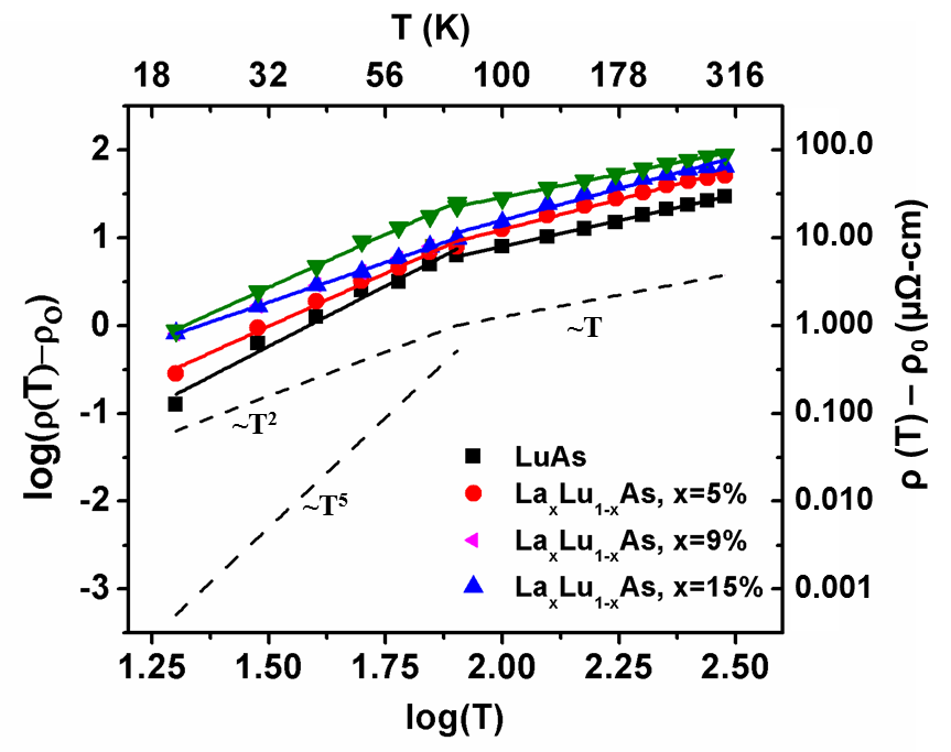
- S. Rahimi, E. M. Krivoy, J. Lee, M. E. Michael, S. R. Bank and D. Akinwande, ” Temperature dependence of the electrical resistivity of LaxLu1-xAs“, AIP ADVANCES, August 2013. (pdf)

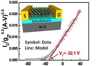
- H.-Y. Chang, S. Yang, J. Lee, L. Tao, W.-S. Hwang, D. Jena, N. Lu and D. Akinwande, “High-Performance, Highly Bendable MoS2 Transistors with High-K Dielectrics for Flexible Low-Power Systems“, ACS Nano, May 2013. (pdf)
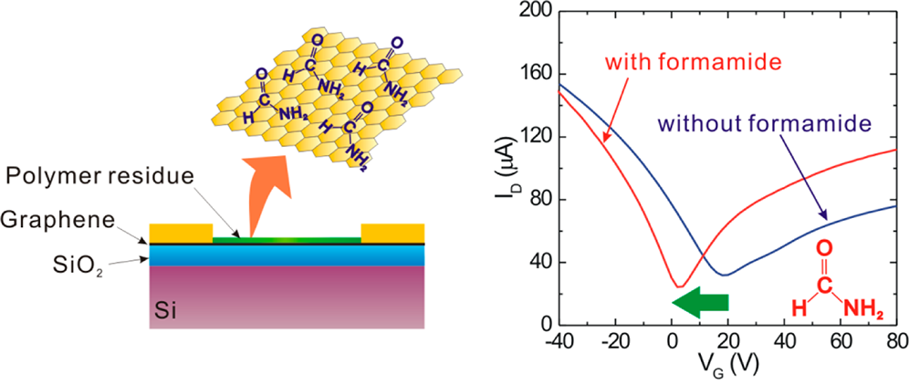
- J. W. Suk, W. H. Lee, J. Lee, H. Chou, R. D. Piner, Y. Hao, D. Akinwande and R. S. Ruoff, “Enhancement of the Electrical Properties of Graphene Grown by Chemical Vapor Deposition via Controlling the Effects of Polymer Residue“, Nano letters, March 2013. (pdf)
- T.-J. Ha, J. Lee, D. Akinwande, and A. Dodabalapur, “The Restorative Effect of Fluoropolymer Coating on Electrical Characteristics of Graphene Field-Effect Transistors“, IEEE Electron Device Letters, March 2013. (pdf)
- J.-Y. Kim, W. H. Lee, J. W. Suk, J. R. Potts, H. Chou, I. N. Kholmanov, R. D. Piner, J. Lee, D. Akinwande, and R. S. Ruoff, “Chlorination of Reduced Graphene Oxide Enhances the Dielectric Constant of Reduced Graphene Oxide/Polymer Composites“, Advanced Materials, Feb 2013.

- J. Lee, T.-J. Ha, K. N. Parrish, Sk. F. Chowdhury, L. Tao, A. Dodabalapur, and D. Akinwande, “High-performance current saturating graphene field-effect transistor with hexagonal boron nitride dielectric on flexible polymeric substrates“, IEEE Electron Devices Letters, vol 34. pp 172 – 174. Feb 2013.
- T.-J. Ha, J. Lee, Sk. Chowdhury, D. Akinwande, P. J. Rossky, and A. Dodabalapur, “Transformation of the Electrical Characteristics of Graphene Field-Effect Transistors with Fluoropolymer“, ACS Appl. Mater. Interfaces, vol 5 issue 1 (January 2013).
2012
- J. Lee, L. Tao, K. N. Parrish, Y. Hao, R. S. Ruoff, and D. Akinwande, “Multi-finger Flexible Graphene Field Effect Transistors with High Bendability”, Appl. Phys. Lett. 101, 252109 (December 2012)
- P. Y. Chen, H. Huang, D. Akinwande, and A. Alu, “Distributed Amplifiers Based on Spindt-Type Field-Emission Nanotriodes,” Nanotechnology, IEEE Transactions on, vol. 11, pp. 1201-1211, 2012.
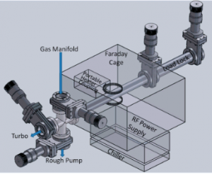
- L. Tao, J. Lee, M. Holt, H. Chou, S. McDonnell, D. Ferrer, M. Babenco, R. Wallace, S. Banerjee, R. Ruoff, and D. Akinwande, “Uniform Wafer-Scale Chemical Vapor Deposition of Graphene on Evaporated Cu (111) Film with Quality Comparable to Exfoliated Monolayer“, The Journal of Physical Chemistry C, vol 116, pp 24068 (October 2012).
- E. M. Krivoy, H. P. Nair, A. M. Crook, S. Rahimi, S. J. Maddox, R. Salas, D. A. Ferrer, V. D. Dasika, D. Akinwande, and S. R. Bank, “Growth and characterization of LuAs films and nanostructures“, Applied Physics Letters, vol. 101, pp. 141910 (2012).
- K. N. Parrish and D. Akinwande, “An exactly solvable model for the graphene transistor in the quantum capacitance limit,” Applied Physics Letters, vol. 101, pp. 053501 (2012).
- T.-J. Ha, D. Akinwande, and A. Dodabalapur, “Hybrid graphene/organic semiconductor field-effect transistors“, Applied Physics Letters, vol. 101, pp 033309 (2012).
- H. Huang, K. Nieman, P. Chen, M. Ferrari, Y. Hu and D. Akinwande, “Properties and Applications of Electrically Small Folded Ellipsoidal Helix Antenna,” IEEE Antennas and Wireless Propagation Letters. vol. 11, pp. 678 – 681 (2012).
- M. Ramon, K. Parrish, S. Chowdhury, C. Magnuson, H. Movva, R. Ruoff, S. Banerjee, and D. Akinwande, “3GHz Graphene Frequency Doubler on Quartz Operating Beyond the Transit Frequency“, IEEE Trans. on Nanotech., vol, 11, pp. 877 – 883 (2012)
- I. N. Kholmanov, M. D. Stoller, J. Edgeworth, W. H. Lee, H. Li, J. Lee, C. Barnhart, J. R. Potts, R. Piner, D. Akinwande, J. E. Barrick, and R. S. Ruff, “Nanostructured Hybrid Transparent Conductive Films with Antibacterial Properties“, ACS Nano, pp. 5157-5163 (2012).
- W. H. Lee, J. W. Suk, H. Chou, J. Lee, Y. Hao, Y. Wu, R. Piner, D. Akinwande, K. S. Kim, and R. S. Ruoff, “Selective-Area Fluorination of Graphene with Fluoropolymer and Laser Irradiation“, Nano Letters, vol. 12, no. 5, pp. 2374 (2012).
- J. Lee, L. Tao, Y. Hao, R. S. Ruoff, and D. Akinwande, “Embedded-gate graphene transistors for high-mobility detachable flexible nanoelectronics“, Applied Physics Letters, vol. 100, pp. 152104 (2012).
- W. H. Lee, J. W. Suk, J. Lee, Y. Hao, J. Park, J. W. Yang, H.-w. Ha, S. Murali, H. Chou, D. Akinwande, K. Kim and R. Ruoff, “Simultaneous transfer and doping of CVD-grown graphene by fluoropolymer for transparent conductive films on plastic”, ACS Nano, vol. 6, no. 2, pp. 1284 (2012).
- L. Tao, J. Lee, H. Chou, M. Holt, R. S. Ruoff and D. Akinwande, “Synthesis of High Quality Monolayer Graphene at Reduced Temperature on Hydrogen-Enriched Evaporated Copper (111) Films”, ACS Nano, vol. 6, no. 3, pp. 2319 (2012).
2011
- K. N. Parrish and D. Akinwande, “Even-odd symmetry and the conversion efficiency of ideal and practical graphene transistor frequency multipliers,” Applied Physics Letters, vol. 99, pp. 223512 (2011).
- L. Tao, J. Lee and D. Akinwande, “Nanofabrication down to 10 nm on a plastic substrate”, J. Vac. Sci. Technol. vol 29, 06FG07 (2011).
- M. Ramon, A. Gupta, C. Corbet, D. Ferrer, H. Movva, G. Carpenter, L. Colombo, G. Bourianoff, M. Doczy, D. Akinwande, E. Tutuc, and S. Banarjee, “CMOS-Compatible Synthesis of Large-Area, High-Mobility Graphene by Chemical Vapor Deposition of Acetylene on Co Thin Films,” ACS Nano, vol. 5, pp. 7198 (2011).
- A. M. Crook, H. P. Nair, J. H. Lee, D. A. Ferrer, D. Akinwande, and S. R. Bank, “Growth of semimetallic ErAs films epitaxially embedded in GaAs“, Proc. of SPIE, vol. 8106 (2011).
- K. N. Parrish and D. Akinwande, “Impact of contact resistance on the transconductance and linearity of graphene transistors,” Applied Physics Letters, vol. 98, pp. 183505 (2011).
Older
- X. Chen, D. Akinwande, K.-J. Lee, G. Close, S. Yasuda, B. C. Paul, S. Fujita, J. Kong and H.-S. P. Wong, ” Fully Integrated Graphene and Carbon Nanotube Interconnects for Gigahertz High-Speed CMOS Electronics,” IEEE Trans. on Electron Devices, vol. 57, pp. 3137 – 3143 (2010).
- D. Akinwande, N. Patil, A. Lin, Y. Nishi, and H.-S. P. Wong, “Surface Science of Catalyst Dynamics for Aligned Carbon Nanotube Synthesis on a Full-Scale Quartz Wafer,” Journal of Physical Chemistry. C, vol. 113, pp. 8002-8008 (2009).
- D. Akinwande, Y. Nishi, and H.-S. P. Wong, “Carbon Nanotube Quantum Capacitance for Non-Linear Terahertz Circuits,” IEEE Trans. on Nanotech., vol. 8, pp 31, (2009).
- D. Akinwande, J. Liang, S. Chong, Y. Nishi, and H.-S. P. Wong, “Analytical Ballistic Theory of Carbon Nanotube Transistors: Experimental Validation, New Device Physics, Parameter Extraction, and Performance Projection,” Journal of Applied Physics, vol. 104, pp. 124514 (2008).
- D. Akinwande, S. Yasuda, B. Paul, S. Fujita, G. Close, and H.-S. P. Wong, “Monolithic Integration of CMOS VLSI and Carbon Nanotubes for Hybrid Nanotechnology Applications,” IEEE Trans. on Nanotechnology, vol. 7, pp. 636-639 (2008).
- J. Liang, D. Akinwande, and H.-S. P. Wong, “Carrier Density and Quantum Capacitance for Semiconduting Carbon Nanotubes,” Journal of Applied Physics, vol. 104, p. 064515 (2008).
- D. Akinwande, Y. Nishi, and H.-S. P. Wong, “An Analytical Derivation of the Density of States, Effective Mass and Carrier Density of Achiral Carbon Nanotubes,” IEEE Trans. on Electron Devices, vol. 55, pp. 289-297 (2008).
- D. Akinwande and H.-S. P. Wong, “A Composite Circuit Model for NDR Devices in Random Access Memory Cells,” IEEE Transactions on Electron Devices, vol. 54, pp. 776-783, 2007.
- D. Akinwande, G. F. Close, and H.-S. P. Wong, “Analysis of the Frequency Response of Carbon Nanotube Transistors,” IEEE Trans. on Nanotech., vol. 5, pp. 599-605, 2006.
- M. Tabib-Azar and D. Akinwande, “Real-time imaging of semiconductor space-charge regions using high-spatial resolution evanescent microwave microscope,” Review of Scientific Instruments, vol. 71, p. 1460, 2000.
- M. Tabib-Azar, D. Akinwande, G. Ponchak, and S. R. LeClair, “Novel physical sensors using evanescent microwave probes,” Review of Scientific Instruments, vol. 70, p. 3381, 1999.
- M. Tabib-Azar, D. Akinwande, G. E. Ponchak, and S. R. LeClair, “Evanescent microwave probes on high-resistivity silicon and its application in characterization of semiconductors,” Review of Scientific Instruments, vol. 70, p. 3083, 1999.
Patents
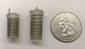
- United States Patent: H. Huang, Y. Hu, and D. Akinwande, “Electrically Small Folded Ellipsoidal/Spherical Helix Antenna for Medical Implant Applications,” Patent Pending, 2012.
- United States Patent: X. Qin, D. Akinwande, J. P. Stephens, R. Zinmaster, and J. Clatterbaugh, “Electrical interconnection for high-frequency devices,” H01P001/04 ed, U. S. Patent Office (2003).